
 Gold Member
 Business License
See the chip clearly and convey trust | Guoyi Quantum Field Emission Scanning Electron Microscope enters CTI CTI Weisibo
See the chip clearly and convey trust | Guoyi Quantum Field Emission Scanning Electron Microscope enters CTI CTI Weisibo
chipAfter an abnormality occurs during R&D, production or use, what customers are most concerned about is not only where the problem is, but also what the problem is.Whether the basis for judgment is sufficient and whether it can support subsequent R&D, mass production or quality decisions.
In failure analysis, testing equipment can provide data; and a conclusion that can be trusted by customers also depends on whether the background of the problem is understood, whether the appropriate analysis path is selected, and whether each judgment can withstand review.
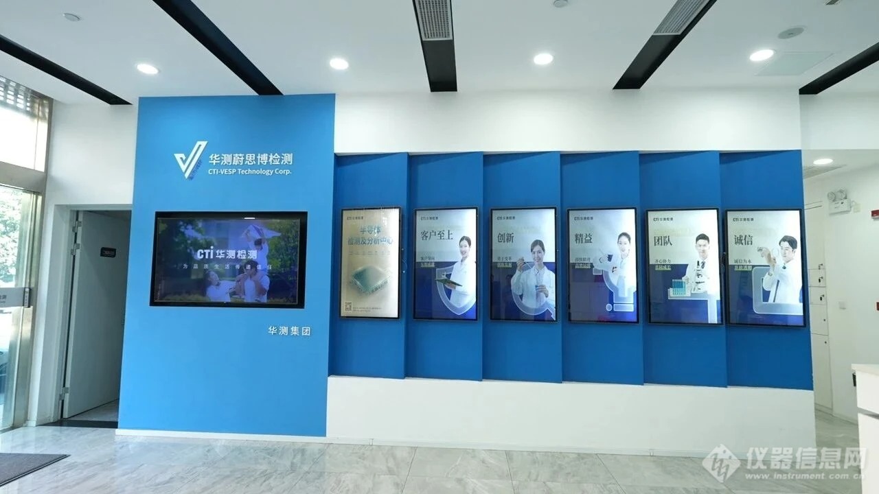
CTI Semiconductor Testing and Analysis Center, carrying out reliability verification, electrostatic protection testing, failure analysis and material analysis for the chip and semiconductor industry. Facing different samples and problems, what the team has to do is sort out the scattered information into technical basis that can support the customer's judgment.
Start with the customer’s problem, not the equipment
A sample sent to the laboratory often carries specific questions during the R&D, production or use process: it may be an abnormality in function, or a problem may be discovered after reliability testing; some customers hope to conduct early destructive analysis to identify risks before mass production.
Dr. Shen Xuan is responsible for the failure analysis and material analysis laboratory management of the Semiconductor Testing and Analysis Center. In his view, analysis does not mean entering a certain piece of equipment immediately after getting the sample, but asking questions clearly first.
Under what conditions does the problem occur? What processes has the sample previously undergone? What information does the customer already have? This seemingly basic information determines where to start the analysis and also affects whether subsequent processing is reasonable.
He likened the job to "doing a doctor on a chip." Just like doctors understand symptoms and medical history, engineers need to first understand the real situation in which the sample is located to avoid going astray at the beginning.
For customers, this step is not only the starting point of analysis, but also the starting point of trust: whether the laboratory truly understands the question determines whether the subsequent data is meaningful.
Base your conclusion on a complete chain of evidence
Failure analysis is not a mechanical process of completing a set of tests in a fixed order. Engineers usually first use non-destructive methods such as appearance observation, X-ray, ultrasonic testing, and electrical IV testing to obtain clues, and determine abnormal areas without damaging the sample as much as possible.
Then based on the existing results, decide whether to open the lid (Decap), remove layers (Delayer) or cross-section preparation (Cross-section)Wait for sample processing, and continue to verify through microscopic morphology observation, component analysis, etc. The previous result provides direction for the next step, and new evidence will in turn verify previous judgments.
What we deliver is not just a photo, but a comprehensive analysis of the failure location, failure mode and possible causes. "Dr. Shen said.
Therefore, an analysis report is more than just a summary of test results. It needs to correlate clues such as sample abnormalities, structure and material information, and process conditions, explain the basis for judgment and possible reasons, and provide customers with reference for subsequent design, process, or quality improvements.
Customer trust comes not only from results
As chip manufacturing processes continue to shrink and structures develop in a three-dimensional direction, failure locations may become more hidden, samples become more precious and more difficult to verify repeatedly. A single device often cannot answer all questions. Different detection and characterization methods need to cooperate and confirm each other, and laboratories also need to establish a stable connection between equipment configuration, engineering experience and cross-link collaboration.
“What customers really need is an analysis result that they can trust, communicate with and support subsequent decision-making,” Dr. Shen said.
This requires engineers to not only understand the technical problems faced by customers, but also to formulate appropriate solutions based on the status of samples; reliability verification, electrostatic protection testing, failure analysis and material analysis also need to be connected as smoothly as possible to reduce the cost of repeated communication and sample delivery by customers.
When problems arise at the R&D or production site, communication and analysis must be advanced simultaneously. Only by providing timely feedback on staged findings and adjusting the path when necessary can the conclusions be returned to the customer's R&D and quality work as soon as possible.
National Instruments Quantum Field Emission Scanning Electron Microscope,Provide support for key evidence
Scanning electron microscopy is a common device used to obtain key evidence in failure analysis. The morphology of the failure point, changes in local structure and elemental composition of related areas often need to be further confirmed through microscopic observation and energy spectrum analysis.
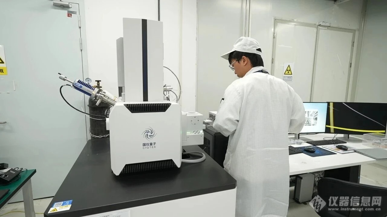
In the Hefei FA laboratory of CTI Weisibo, Guoyi Quantum SEM4000X field emission scanning electron microscope undertakes a large number of cross-sectional analysis and surface analysis tasks. The equipment is equipped with energy spectrum analysis function for morphology observation and micro-component analysis.
existCTI WeisiboShanghaiFAIn the laboratory, the Guoyi Quantum SEM5000X field emission scanning electron microscope is equipped with a nanoprobe station. In addition to high-resolution morphology observation, more refined micro-region electrical analysis can also be carried out to supplement electrical information for complex samples.
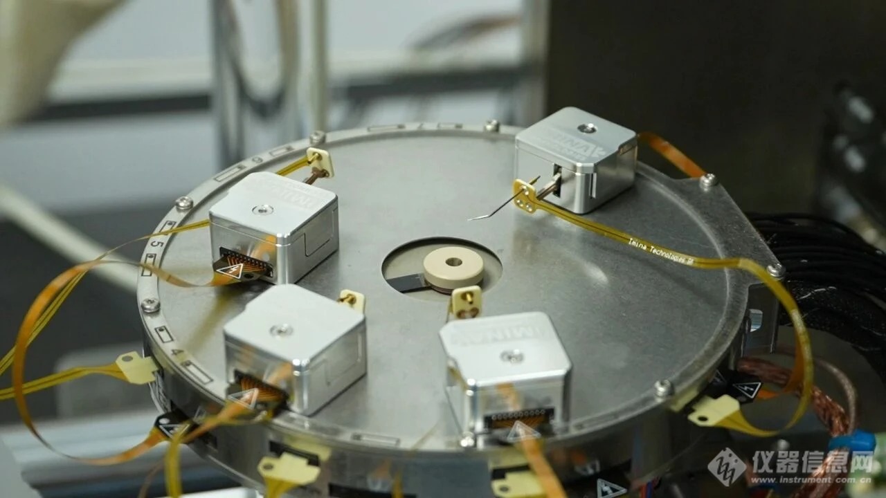 Partial close-up of nanoprobe station
Talking about daily use experience, Dr. Shen said that the progress of domestic field emission scanning electron microscopes in recent years is "real" and the equipment is "very stable and very convenient." For laboratories, the value of this type of equipment lies in putting key observation and verification links into a continuous, executable analysis path.
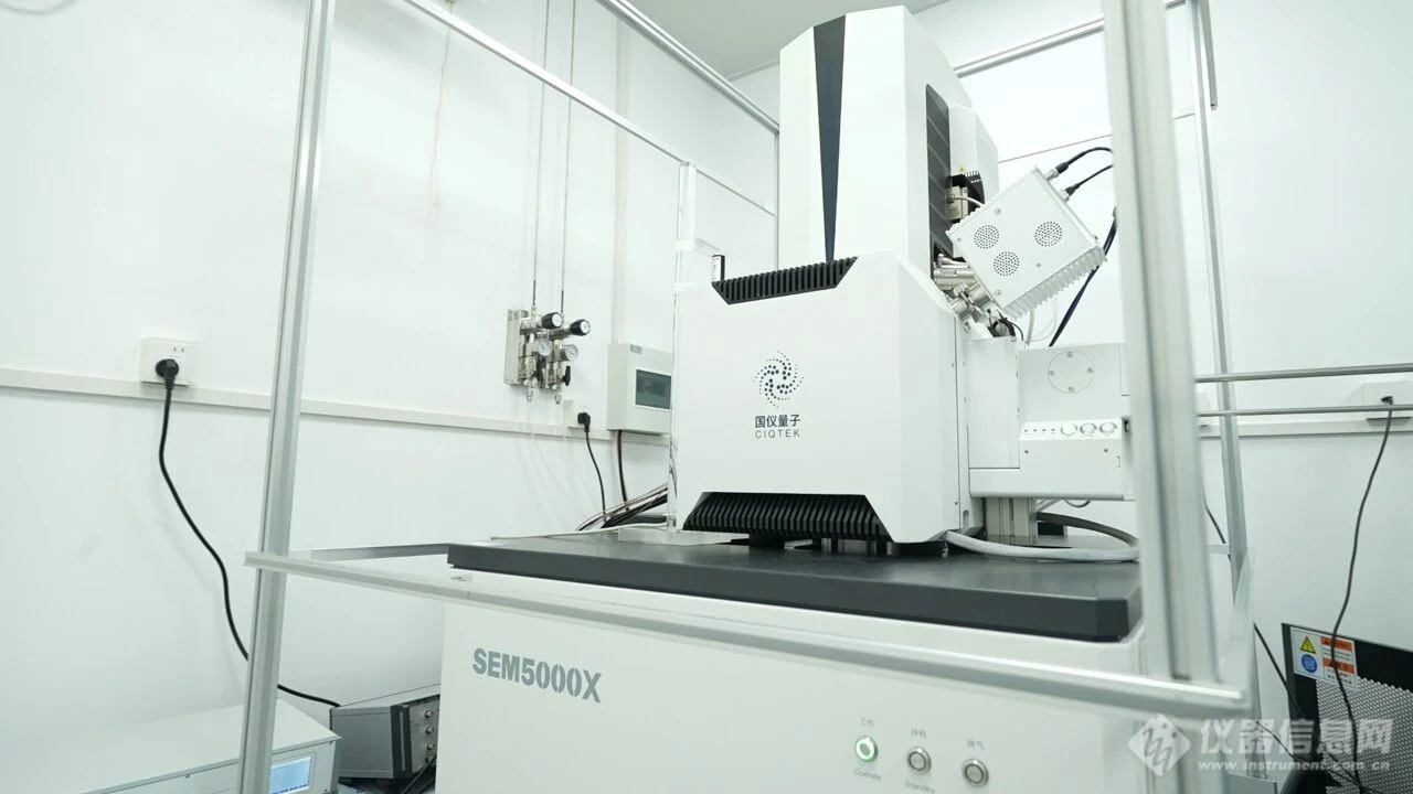 Guoyi Quantum SEM5000X field emission scanning electron microscope in CTI Weisibo Shanghai FA laboratory
Deliver reviewable conclusions to clients
The value of the detection industry is not just about discovering an anomaly, but also about allowing customers to understand how the conclusion was formed and what can be done next.
The testing industry is an industry that conveys trust. This trust comes from a careful understanding of customer problems, from full communication during the analysis process, and from the clear and reviewable relationship between each piece of data and judgment.
In the future, CTI Weisibo will continue to improve its failure analysis capabilities based on the actual needs of customers, expand the methods and applications of material analysis, and strengthen the cooperation between different detection methods. Make the analysis process more complete, the data and conclusions more intuitive and transparent, and ultimately serve customers' research and development, quality judgment and subsequent improvements.
View More from This Booth

"Nature Materials"! How is graphene magnetism “seen”? Guoyi Quantum SNVM helps customers realize graphene spin

Guoyi Quantum Scanning Electron Microscope helps high-performance sodium ion batteries! Uncovering the stabilization mechanism of layered oxide cathodes
Give the knob to AI and leave the judgment to you|Guoyi Quantum Electron Microscope AI Agent